The iSMART (innovation in Surfaces, MAterials and Related Technologies) research group [part of the Medical Technologies Innovation Facility (MTIF), Nottingham, UK] focusses their research interest around the optical and electronic properties of materials and thin films for nano-photonic and electronic applications. One such example of a family of materials related to both applications areas is the metal oxides. Metal oxides have emerged as promising material candidates in various electronic and optoelectronic applications offering unique advantages such as high mobility, wide bandgap (transparent in the visible range) and the ability to be controllably doped. Importantly, iSMART has developed routes to different scalable deposition techniques for such materials (from wet chemistry methods to vacuum deposition techniques).
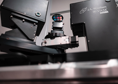
Spectroscopic ellipsometry (SE) is a highly sophisticated and non-destructive metrology tool for determining the optical constants of materials. iSMART is equipped with a J.A. Woollam Infrared Variable Angle Spectroscopic Ellipsometer (IR VASE II), capable of providing the optical constants of materials in the extended spectral range from 1.6 µm to 40 µm.
Supplier of the IR VASE II, Quantum Design UK and Ireland Ltd, and MTIF have entered into a partnership to provide access to potential users to view, and measure trial samples on, the ellipsometer on an ad hoc contract basis. In partnership with The University of Nottingham, this spectral range can be extended further, using a J.A. Woollam M-2000DI spectroscopic ellipsometer, to include the near infrared, visible and ultraviolet wavelengths (1.69–0.193 µm). This combined capability provides one of the widest spectral ranges available (0.19–40 µm). By extracting the exact optical constants, material properties such as charge transport (mobility, doping concentration, resistivity), lattice vibration (phonon absorption) and band structure (via interband transitions and band gaps) can also be determined.
These fundamental properties of semiconducting materials are key parameters for opto–electronic applications. Recently, Dr Nikolaos Kalfagiannis and co-workers from Université de Poitiers, Sheffield Hallam University and The University of Nottingham have employed SE in the extended spectral range (0.2–40 µm) and developed the methodology for the accurate determination of the free carrier transport properties of transparent conductive oxides and the ability to discriminate between the different scattering mechanisms (grain boundary scattering, inter-grain scattering and ionised impurity scattering) in an effort to clarify the conduction mechanisms of such materials and define their range of application.

