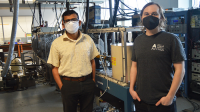
Researchers from the Positron Lab in the University of Texas at Arlington (UTA) Department of Physics utilised a process called Auger-mediated positron sticking (AMPS) to develop a novel spectroscopic tool to measure the electronic structure of the surface of materials selectively. The AMPS process, in which positrons (antimatter of electrons) stick directly to surfaces followed by electron emission, was first observed and described by Saurabh Mukherjee, a graduate student, along with Alex Weiss, professor and chair of the UTA Department of Physics, and other colleagues in 2010 at UTA.
“Alex (Fairchild) and Varghese figured out how to use this phenomenon that we discovered in 2010 to measure the top layer and get information about the electronic structure and the behaviour of the electrons in the top layer”, Weiss said. “That will determine a material’s many properties, including conductivity, and can have important implications for building devices.”
Alex Fairchild, postdoctoral scholar in the Positron Lab, said the AMPS process is unique because it uses virtual photons to measure the top-most atomic layer. “This is different from typical techniques like photoemission spectroscopy, where a photon penetrates multiple layers into the bulk of a material and therefore contains the combined information of the surface and subsurface layers”, he said.
“Our AMPS results showed how virtual photons emitted following positron-sticking interact preferably with electrons that extend further into the vacuum than with electrons that were more localised to the atomic site”, Varghese Chirayath, assistant professor of research, said. “Our results are thus essential to understand how positrons interact with surface electrons and are extremely important to understand other similarly surface-selective, positron-based techniques.”


