Articles
Raymond J. Abraham and Mehdi Mobli
Chemistry Department, The University of Liverpool, PO Box 147, Liverpool L69 3BX, UK
Phillip R. Greene and Colin D. Bain
Department of Chemistry, University of Oxford, Chemistry Research Laboratory, Mansfield Road, Oxford, OX1 3TA, UK
Steve Down
HD Science Limited, 16 Petworth Avenue, Toton, Nottingham NG9 6JF, UK
Richard A. Crocombe
Axsun Technologies, Inc., 1 Fortune Drive, Billerica, MA 01821, USA
J. Mortona and Simon M. Nelmsb
aBiological Monitoring, Health and Safety Laboratory, Broad Lane, Sheffield, S3 7HQ, UK
bThermo Electron Corporation, Ion Path, Road Three, Winsford, Cheshire, CW7 3BX, UK
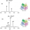
In recent years, the newly-developed soft ionisation techniques together with the possibility to measure masses by high-resolution mass analysers with high transmission and with a broad mass-to-charge range have given mass spec-trometry the opportunity to add complementary information to the protein structural biology community.
Peter Wilhelm,a Boril Chernev,a Peter Pölt,a Gerald Kothleitner,a Klaus-Jochen Eichhorn,b Gisela Pompe,b Nikola Johnerc and Alexander Piryc
aResearch Institute for Electron Microscopy, Graz University of Technology; Steyrergasse 17, A-8010 Graz, Austria. E-mail: [email protected]
bInstitute of Polymer Research Dresden; Hohe Straße 6, D-01069 Dresden, Germany
The goal of building a multivariate calibration model is to predict a chemical or physical property from a set of predictor variables, e.g. analyte concentration or octane number from a near infrared (NIR) spectrum. A good multivariate calibration model should be able to replace the laborious, possibly imprecise reference method. The quality of a model therefore primarily depends on its predictive ability. Other properties such as interpretability of the model coefficients might also be of interest, but here the focus is on the problem of quantifying the predictive ability.
Gabriel Pinto and Isabel Paz
Departamento de Ingeniería Química Industrial y del Medio Ambiente, E.T.S.I. Industriales, Universidad Politécnica de Madrid, José Gutiérrez Abascal 2, 28006 Madrid, Spain
Philippe Colomban
LADIR-UMR 7075 CNRS & Université P. & M. Curie, 2 rue Henry Dunant, 94320 Thiais, France
Paul Dumas
LURE, centre Universitaire Paris Sud, BP 34, F-91898 Orsay Cédex, France
Mark J. Tobin
CCLRC Daresbury Laboratories, Warrington, Cheshire WA4 4AD, UK
E.A.H. Timmermans and J.J.A.M. van der Mullen*
Department of Applied Physics, Eindhoven University of Technology, PO Box 513, 5600 MB Eindhoven, The Netherlands. E-mail address [email protected]
G.J. Price, G.W. Fraser, J.F. Pearson, I.B. Hutchinson, A.D. Holland, J. Nussey, D. Vernon, D. Pullan and K. Turner
Space Research Centre, Department of Physics and Astronomy, University of Leicester, Leicester LE1 7RH, UK. E-mail: [email protected]
David Chenery and Hannah Bowring
Smith & Nephew Group Research Centre, York Science Park, Heslington, York YO10 5DF, UK
T. Wirtz and H.-N. Migeon
Laboratoire d’Analyse des Matériaux, Centre de Recherche Public - Gabriel Lippmann, 162A, av. de la Faïencerie, L-1511 Luxembourg, [email protected]
Luisa Mannina,a,b Anatoli P. Sobolevb and Annalaura Segreb
aUniversity of Molise, Faculty of Agriculture, 86100 Campobasso, Italy
bInstitute of Chemical Methodologies, CNR, 00016 Monterotondo Staz., Rome, Italy
Introduction
Glow Discharge Mass Spectrometry (GDMS) is one of the most powerful solid state analytical methods for the direct determination of traces, impurities and depth profiling of solids.1–5 Glow discharge mass spectrometers, which are commercially available with fast and sensitive electrical ion detection, allow direct trace elemental determination in solid materials with good sensitivity and precision in the concentration range lower than ng g–1.6
Moore’s law* dictates microelectronics researchers to make integrated circuit (IC) devices smaller and to put them as close to each other as possible on a chip. This results in a better performance and a larger functionality of the chips. However, these devices also require a good electrical isolation from each other. This is in general done by the formation of a thick local oxide in the “field region” between the devices. In 1970, researchers from Philips1 invented the so-called LOCOS (LOCal Oxidation of Silicon) technique to achieve this isolation. Using a Si3N4 mask, the silicon is thermally oxidised in the nitride-free field regions. Figure 1 (left) shows a typical LOCOS structure. Although LOCOS seemed a perfect solution at that time, it came with a lot of problems, many of them related to mechanical stresses. Thermal oxidation of Si to SiO2 occurs together with a 125% volume expansion. As a result, the oxide grown in the field region, called the “field oxide,” exerts large forces on the surrounding silicon. Another major drawback of this technique is the so-called “bird’s beak,” caused by the lateral growth of the oxide under the nitride mask. This bird’s beak not only affects the intended device length, it also introduces large local mechanical stresses in the silicon, because of volume expansion, and it also deforms the nitride film. These stresses often resulted in the generation of dislocations in the silicon, which are quite harmful for the devices.
Alan Street
Technical Director, Oxford Instruments Superconductivity
S.Y. Luk,a N. Patela and M.C. Daviesb
aMolecular Profiles Ltd, 1 Faraday Building, Nottingham Science & Technology Park, University Boulevard, Nottingham NG7 2QP, UK. E-mail: [email protected]
bLaboratory of Biophysics and Surface Analysis, School of Pharmaceutical Sciences, University of Nottingham, Nottingham NG7 2RD, UK


