Ingrid De Wolf
IMEC, Kapeldreef 75, B-3001 Leuven, Belgium
Introduction
Stress in microelectronics
Moore’s law* dictates microelectronics researchers to make integrated circuit (IC) devices smaller and to put them as close to each other as possible on a chip. This results in a better performance and a larger functionality of the chips. However, these devices also require a good electrical isolation from each other. This is in general done by the formation of a thick local oxide in the “field region” between the devices. In 1970, researchers from Philips1 invented the so-called LOCOS (LOCal Oxidation of Silicon) technique to achieve this isolation. Using a Si3N4 mask, the silicon is thermally oxidised in the nitride-free field regions. Figure 1 (left) shows a typical LOCOS structure. Although LOCOS seemed a perfect solution at that time, it came with a lot of problems, many of them related to mechanical stresses. Thermal oxidation of Si to SiO2 occurs together with a 125% volume expansion. As a result, the oxide grown in the field region, called the “field oxide,” exerts large forces on the surrounding silicon. Another major drawback of this technique is the so-called “bird’s beak,” caused by the lateral growth of the oxide under the nitride mask. This bird’s beak not only affects the intended device length, it also introduces large local mechanical stresses in the silicon, because of volume expansion, and it also deforms the nitride film. These stresses often resulted in the generation of dislocations in the silicon, which are quite harmful for the devices (see Figure 1).
*Moore’s law: this is attributed to an observation in the mid-1960s made by Gordon Moore, cofounder of Intel, that the number of transistors per square inch on ICs had doubled since the technology was invented. He predicted the trend would continue for the foreseeable future.
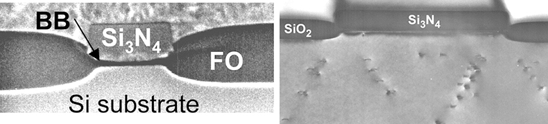
Figure 1. TEM pictures showing a LOCOS structure. Left: field oxide (FO) and bird’s beak (BB) are indicated. Right: stress induced dislocations in the Si-substrate.
Measuring these local stresses using known techniques such as wafer bending or x-ray diffraction (XRD) was not possible at that time. The devices were too small (µm size). So, in the 1980s and beginning of the 1990s, a lot of effort was spent on simulation of the oxidation process, the LOCOS formation and the induced stresses. However, this simulation process was not straightforward. The different materials had to be treated as being non-linear visco-elasto-plastic, their material parameters could change with temperature and stress, and the oxidation rate depended on the (changing) silicon crystal orientation. Although this seemed a mission impossible, many researchers succeeded in simulating the LOCOS process quite well. But this did not really solve the questions on stress. How large is this stress, what is the effect of processing parameters and materials used, and what is the effect of geometry? Answering these questions is why Raman spectroscopy found much greater utilisation within the microelectronics industry.
Raman spectroscopy and microelectronics
Raman spectroscopy was of course already being used in the 1970s for the study of semiconductors. It allows identification of the material and yields information about phonon frequencies, energies of electron states and electron–phonon interaction, carrier concentration, impurity content, composition, crystal structure, crystal orientation, temperature and mechanical strain.2
Several studies on the effect of strain on the Raman signal of semiconductors were initiated in Germany by Professor Cardona’s group at the Max-Planck Institute for Solid State Research, Stuttgart, and further investigated in detail by Professor E. Anastassakis.3 Strain in the crystal affects the frequency of the phonons, and as such the position of the Raman peak. In 1980, this property was exploited in the microelectronics industry, but only for uniform films: Raman spectroscopy was applied to measure the stress in silicon films on sapphire substrates.4 In 1983, researchers from Mitsubishi Electronic Corporation in Japan used micro-Raman spectroscopy to study the recrystallisation and crystal orientation of silicon with a high spatial resolution.5,6 This work triggered Japanese researchers from Toshiba Corp. to use Raman spectroscopy for the measurement of local stress.7 They applied the technique to study stress in and outside grooves etched in Si. They measured a Raman spectrum of Si at one point in between grooves with different spacing, and related the frequency differences to differences in local stresses.
In 1987, the Mitsubishi group8,9 showed that micro-Raman spectroscopy could be used to measure mechanical stress in the Si near LOCOS structures with a spatial resolution of about 1 µm. They did not just measure at single points, but performed scans along equidistant points (1 µm) along a line, as shown in Figure 2.
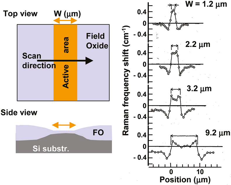
Figure 2. Left: schematic showing the measurement position, Right: Raman frequency shift for LOCOS with different widths.8
Once it was proved that Raman spectroscopy could be used to measure local stresses in Si devices, application of the technique became popular very quickly in microelectronics research centres and industry.
In IMEC (Interuniversity MicroElectronics Center), Belgium, we started using this technique for the study of stress in LOCOS in 1989. This was soon followed by measurements on alternative isolation schemes such as LOPOS (Polysilicon-buffered LOCOS) and PELOCOS (Polysilicon encapsulated LOCOS),10–13 shallow and deep trench isolation,14 silicides15 and even MEMS (MicroElectroMechanical Systems),16 solder bumps and packaged chips.17 The technique also evolved during these years. The measurements in 1989 were rather cumbersome: one had to move the X–Y stage by hand or joystick, focus the probing laser beam on the sample, start the measurement, save the data, move the X–Y stage again etc. This took a lot of patience and time. Now, you just put the sample at the correct position, define the measurement area and the computer does it all for you: autofocus, moving the stage, saving the data, fitting the spectra etc.
Below we show some typical results of local stress measurements in microelectronics structures, performed using micro-Raman spectroscopy. They demonstrate the unique possibilities and the power of the technique for this application.
Raman spectrum of silicon
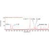
Figure 3 shows a typical Raman spectrum of crystalline silicon. The sharp, Gaussian-like lines which can also be seen in the spectrum shown in Figure 3 are Rayleigh scattered plasma lines from the argon laser. They can be used for calibration.
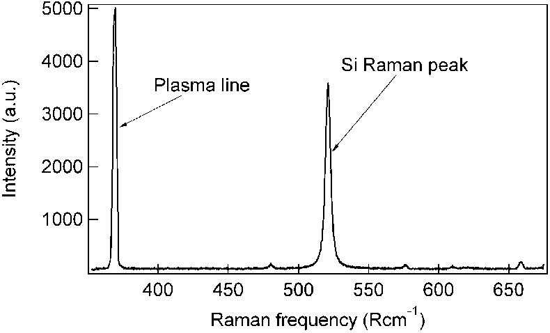
Figure 3. Typical Raman spectrum of crystalline silicon, measured using the 457.8 nm line of an argon laser. It shows the Si Raman peak and plasma lines from the laser.
The Raman scattering frequency of Si is at ω = 521 Rcm–1, however, mechanical strain results in a change of this value. By monitoring this frequency at different positions on the sample, a “strain map” can be obtained with micrometer spatial resolution. Raman instruments dedicated for stress measurements are able to measure frequency changes as small as 0.02 cm–1. For silicon, this corresponds with a stress sensitivity of about 10 MPa.
The relation between strain or stress and the Raman frequency is rather complex.3,11 All non-zero strain tensor components influence the position of the Raman peak. In some cases, however, the relation becomes simply linear. For example, for uniaxial (σ) or biaxial (σxx + σyy) stress in the (100) plane of silicon, this relation is:
σ (MPa) = –435 Δω (cm–1)
or
σxx + σyy (MPa) = –435 Δω (cm–1)
(1)
In general, compressive stress will result in an increase of the Raman frequency, while tensile stress results in a decrease. However, if more complex strain pictures are expected, such as for example at the edge of a film, or near a trench or LOCOS structure, the relation between Δω and the strain tensor components is more complicated. In order to obtain quantitative information on the strain in this case, some prior knowledge of the strain distribution in the sample is required. In other words, one has to presuppose a strain model. From this model, the expected Raman shift can be calculated and compared with the Raman data, and feedback can be given to the model. Of course, some experimental parameters, such as the penetration depth of the laser light in the sample and the diameter of the focused laser beam on the sample have to be taken into account.
Stress measurements
Nitride lines
The first example shows results from stress measurements on very simple structures: long Si3N4 stripes with different widths on a silicon substrate. These nitride lines are under tensile stress due to the deposition process. As a result, they compress the Si atoms in the substrate under them causing compressive stress, and they pull at the Si atoms next to the lines, causing tensile stress. This effect is clearly seen in the Raman spectroscopy data of Figure 4.
This figure shows the measured shift of the frequency of the Si Raman peak when scanning along a line across the width of such stripes.12 The position of the stripes is indicated by the lines on top of the data. The laser is first focused far from the lines, where the stress can be assumed to be zero. Next the sample is moved, using the XY-stage, in steps of 0.1 µm and at each position a Si-Raman spectrum, such as the one shown in Figure 3, is recorded. A Lorentzian function is fitted to each of these Raman peaks in order to determine the frequency. The shift of this frequency from the stress free value, Δω, is plotted as a function of the position on the sample where the corresponding spectrum was measured. Figure 4 shows that Δω becomes negative when approaching the lines, indicating tensile stress (Equation 1). When crossing the border, Δω changes sign very fast to reach a maximum positive value under the line, near the edge, indicating compressive stress. Δω remains positive under the line, with some relaxation towards the centre. In order to obtain an idea about the magnitude of the stress, one can assume uniaxial stress, σ, along the width of the line. This assumption is not too bad near the centre of the line, but it does not hold at the edges. A shift of Δω = 0.2 cm–1, as measured in the silicon under the centre of the wide nitride line, would then correspond with a compressive stress of about –90 MPa. This stress clearly increases with decreasing width of the Si3N4 lines. It becomes about –300 MPa for 2.5 µm wide lines. It is possible to obtain more detailed information on the different stress components by fitting a stress model to the Raman data.12 This was done for these nitride lines using the so-called analytical “edge force model.”18 The full lines in Figure 4 show the result of a fit of this model to the µRS (micro-Raman spectroscopy) data, taking into account experimental parameters such as probing spot diameter and penetration depth. This procedure of fitting theoretical stress models to Raman data can be used for any model describing any device where Raman data can be measured. In this way, µRS can be used to experimentally verify stress models.
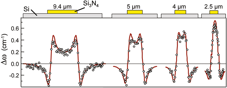
Figure 4. Δω (symbols) measured on nitride lines with different widths on Si substrate. The rectangles at the top indicate the position of the lines. See text for details.
Silicides
Stress induced in Si by metal lines can also be studied. Figure 5 shows the result of a µRS scan across a Si sample with arrays of [110] oriented 16 nm thick TiSi2 lines with decreasing pitch.19,20 The position of the TiSi2 lines is indicated by the stripes on Figure 5. TiSi2 lines do give a Raman signal, but this signal is very weak and difficult to use for the monitoring of stress in the lines. It can be used, however, to study the phase of the TiSi2.21 In this study, we measured the stress induced by the silicide lines in the silicon substrate next to the lines, and the effect of line pitch on this stress. The laser light could not penetrate through the silicide, so, no signal is obtained from underneath the lines.
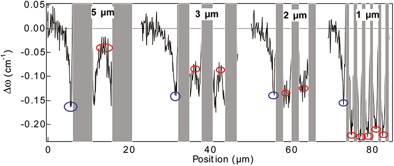
Figure 5. Shift of the silicon Raman peak, Δω, from the stress free frequency as a function of the position on 16 nm thick TiSi2 lines, spacing = width = 5, 3, 2 or 1 µm, on (100) Si substrate.
Δω becomes negative near the edge of the lines (blue circles), indicating the presence of tensile stress in the silicon (Equation 1). In between the lines (red circles), Δω remains negative. For smaller spacing between the lines, this negative value of Δω increases, showing that the tensile stress in between the lines increases with decreasing spacing. From this experiment one can expect that for a certain line spacing, this tensile stress might become so large that it will trigger the formation of dislocations. TEM analysis of 110 nm thick TiSi2 lines showed that dislocations indeed start to occur in the silicon when the spacing was equal to or smaller than 1 µm.
Isolation
As mentioned in the introduction, an important processing step is the isolation of active areas in Si chips. This isolation, through the growth of a LOCOS, or through the etching and oxide-filling of shallow or deep trenches, is known to induce large stress in the silicon substrate. Figure 6 show the result of two Raman experiments performed during a two-dimensional scan across a 3 µm wide square (left) and line (right) active Si isolated by PBLOCOS (Poly-buffered LOCOS). The stress is tensile (Δω < 0) near the edges and compressive (Δω > 0) in the centre. Notice that the tensile region is larger near the sides of the square than near the edges. On the other hand, the compressive stress is larger at the edges of the square and of the line than near the sides, and there is also a clear relaxation towards the centre. These experiments demonstrate the stress-mapping capabilities of micro-Raman spectroscopy.
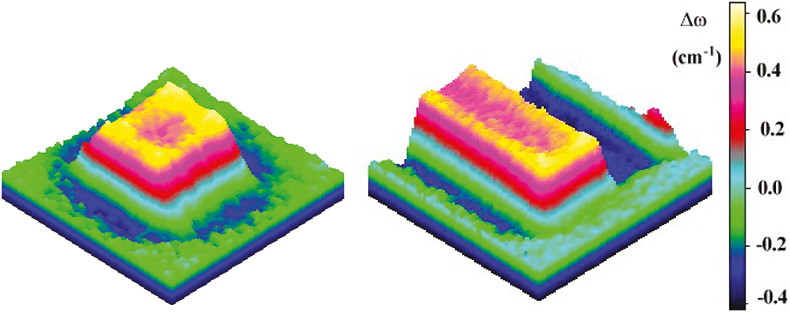
Figure 6. Shift of the silicon Raman peak, Δω, from the stress free frequency as a function of the position on 3 µm wide active square Si region (left) and line (right) isolated by PBLOCOS.22
Packaging
When information on the variation of stress with depth has to be obtained, there are three possible ways to proceed. The first is by changing the probing depth by using different wavelengths of the exciting laser. A disadvantage of that approach is that the Raman signal arises from the whole probed area. This can be minimised by making use of the confocality of the system. This works well in transparent samples, like GaN or diamond, but is not so useful in opaque samples such as silicon. A third way is to cleave the sample, and polish if required, and to measure on the cross-section. An example of this last approach is shown in Figure 7.
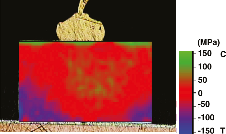
Figure 7. Stress in a Si chip bonded to a Cu substrate.17
The packaging process of chips, including wire bonding, solder bumping, chip adhesion to a substrate, glob top covering etc. also introduces stresses in the chip. These stresses are in general studied through finite element (FE) simulations, but they can in many cases also be studied using Raman spectroscopy. Figure 7 shows the example of a stress map, measured by Raman spectroscopy on the cross-section of a Si chip that was bonded to a copper substrate.17 Due to the difference in thermal expansion coefficient between Si and Cu, this bonding induces stresses in the silicon. One can clearly distinguish stresses introduced by both the Cu substrate and the solder bump on the top of the chip. This kind of study allows the comparison of stress introduced by different chip/substrate bonding processes, the effect of encapsulation of the chips, and even the effect of changes in the wire bonding process.
MEMS: pressure sensor membrane
As a last example, we discuss a µRS experiment on the Si membrane of a pressure sensor.16 This sensor was processed by etching cavities in the silicon wafer and bonding the wafer anodic to a glass substrate [Figure 8(a)]. The bonding introduced a negative pressure under the membrane, resulting in an inward deflection of about 5 µm. A µRS-system equipped with an autofocus module was used to scan the surface of the membrane. Figure 8(b) shows the mechanical stress in the membrane, calculated from the change of the Raman frequency (Δω) from its stress free value, assuming biaxial stress. We clearly find compressive stress in the centre of the membrane and tensile stress near the sides. The corners have very low stresses. Similar experiments were performed on the underside of the membrane. Indeed, the µRS-technique allows probing of the silicon through the glass substrate. This makes it possible to study, for example, the glass/silicon interface.
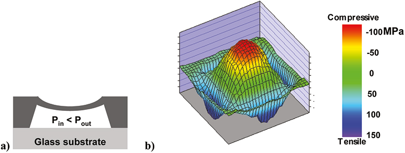
Figure 8. (a) Schematic showing the membrane on glass substrate. (b) Mechanical stress in a 4 mm × 4 mm membrane measured using Raman spectroscopy. The stress is calculated assuming biaxial stress in the membrane.16
Conclusions
Mechanical stress has always been an important concern for IC-processing and reliability engineers. This stress occurs at nearly all the stages of the chip development and life: during deposition of films, temperature steps, oxide growth, silicidation, trench filling, wafer thinning, dicing, chip bonding, chip packaging and in an environment with ever changing temperatures.
Mechanical stress can have direct or indirect effects on the functioning and reliability of a chip, and cause different failure modes, such as changes in electron or hole mobility, dislocations near LOCOS (Figure 1) or trench isolation structures giving rise to an increased leakage current, dislocations near dense silicide lines, fracture of MEMS, cracks in chips, breaking of solder bumps, creep in metals, stress migration etc.
S.M. Hu correctly predicted in 1991:18 “Many problems of defective devices in silicon ICs can be traced ultimately to stresses that develop at various stages of IC processing. These problems will become more acute as IC devices become more complex in geometry and material mix.” The same can be said for IC packages.
It is important to control mechanical stress induced by processing steps in IC and MEMS manufacturing and chip packaging. The stress can in many cases be monitored using micro-Raman spectroscopy. This technique is rather unique in the sense that it is the only simple, spectroscopic, non-destructive technique that can offer this information. Only examples from Si devices were shown, but Raman spectroscopy is not restricted to Si. For example, the technique can also be applied to semiconductor materials such as Ge, GaAs, GaN etc.
Acknowledgements
The examples used in this paper came from collaboration with different people: many thanks to Veerle Simons, Merlijn van Spengen, Chen Jian, Ann Steegen, Dave Howard, Karen Maex, Rita Rooyackers and Goncal Badenes.
References
- J.A. Appels, E. Kooi, M.M. Paffen, J.J.H. Schatorji and W.H.C.G. Verkuylen, Philips Res. Rep. 25, 118 (1970).
- M. Cardona, SPIE 822, 2 (1987).
- E.M. Anastassakis, “Morphic effects in lattice dynamics,” in Dynamical Properties of Solids, Ed by G.K. Horton and A.A. Maradudin. North-Holland Publishing Company (1980).
- Th. Englert, G. Absteiter and J. Pontcharra, Solids State Electronics 23, 31 (1980).
- S. Nakashima, Y. Inoue, M. Miyauchi and A. Mitsuishi, J. Appl. Phys. 54, 2611 (1983).
- S. Nakashima, Y. Inoue and A. Mitsuishi, J. Appl. Phys. 56, 2989 (1984).
- S. Kambayashi, T. Hamasaki, T. Nakakubo, M. Watanabe and H. Tango, Extended abstracts of the 18th conference on Solid State Devices and Materials, pp. 415–418 (1986).
- K. Kobayashi, Y. Inoue, T. Nishimura, T. Nishioka, H. Arima, M. Hiroyama and T. Matsukawa, Extended abstracts of the 19th conference on Solid State Devices and Materials, Tokyo, pp. 323–326 (1987).
- Y. Inoue, T. Nishimura and Y. Akasaka, Mitsubishi Electric Advance 41, 28 (1987).
- A. Romano-Rodriguez, J. Vanhellemont, I. De Wolf, H. Norstrom and H.E. Maes, TEM study of LOPOS structures for submicron isolation. Inst. Phys. Conf. Ser. No. 117, Section 4, pp. 165–168 (1991).
- I. De Wolf, Topical Review, Semicon. Science & Technol. 11(2), 139 (1996).
- I. De Wolf, H.E. Maes and S.K. Jones, J. Appl. Phys. 79(9), 7148 (1996); I. De Wolf and E. Anastassakis, “Addendum”, J. Appl. Phys. 85(10), 7484 (1999).
- G. Badenes, R. Rooyackers, I. De Wolf and L. Deferm, “Polysilicon encapsulated LOCOS for deep submicron CMOS lateral isolation,” Ext. Abstracts of the 1996 Int. Conf. On Solid State Devices and Materials, Yokohama, pp. 46–48 (1996).
- I. De Wolf, G. Groeseneken, H.E. Maes, M. Bolt, K. Barla, A. Reader and P.J. McNally, Conf. Proc. 24th International Symposium for Testing and Failure Analysis (ISTFA), ASM Intn., pp.11–15 (1998).
- A. Steegen, K. Maex and I. De Wolf, Local mechanical stress induced defects for Ti and Co/Ti silicidation in sub-0.25 µm CMOS technologies. IEEEVLSI symposium, pp. 200–201 (1998).
- W.M. van Spengen, I. De Wolf and R. Knechtel, Proc. SPIE Micromachining and Microfabrication, Sept. 2000.
- C. Jian and I. De Wolf, Proc. 3th Electronics Packaging Technology Conference (EPTC2000), Singapore (2000).
- S.M. Hu, J. Appl. Phys. 70(6), (1991).
- I. De Wolf, D.J. Howard, K. Maex and H.E. Maes, Mat. Res. Soc. Symp. Proc. Vol. 427 (1996).
- A. Steegen, I. De Wolf and K. Maex, J. Appl. Phys. 86(8), 4290 (1999).
- I. De Wolf, D.J. Howard, A. Lauwers, K. Maex and H.E. Maes, Appl. Phys. Lett. 70(17), 2262 (1997).
- I. De Wolf, J. Raman Spectrosc. 30, 877 (1999).