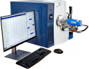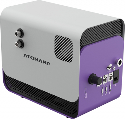
Atonarp has announced the launch of Aston, an in situ mass spectrometer with an integrated plasma ionisation source for semiconductor metrology. Aston has been built for semiconductor production, and can replace multiple legacy tools and provide control across a number of applications, including lithography, dielectric and conductive etch and deposition, chamber clean, chamber matching, and abatement. Endpoint detection (EPD) is the most efficient way to run a semiconductor tool and FAB. EPD has not been able to be deployed in many process steps because the required in situ sensor would not survive the harsh process or chamber cleaning chemicals, or would alternatively suffer clogging from condensate deposits. FABs have had to use a fixed time to ensure that a process was complete. Aston optimises production by detecting exactly when a process has finished, including chamber cleaning, which can reduce the required clean-time by up to 80 %. Aston is resistant to corrosive gases and gaseous contaminant condensates. It has independent dual ionisation sources, a classic electron impact ionisation source and a filament-less plasma ioniser, that work reliably in the harsh conditions encountered in semiconductor production. This enables Aston to be used in environments where traditional electron ionisers would corrode and fail very rapidly.
Aston offers an interval between service events that is up to 100× longer than legacy mass analysers. It includes self-cleaning capability that eliminates the build-up resulting from the deposition of condensates present in certain processes. Since Aston generates its own plasma, it works with or without process plasma present. This provides an advantage over optical emission spectroscopy techniques, which require a plasma source to operate, making Aston ideal for ALD and certain metal deposition processes that may use a weak, pulsed or no plasma for processing.


