

A team of researchers at the Institute of Laser Engineering, Osaka University, in collaboration with Bielefeld University and Technical University Braunschweig in Germany, have come closer to unravelling the complicated optical response of wide-bandgap semiconductor multiple quantum wells and how atomic-scale lattice vibration can generate free space terahertz emission. Their work provides a significant push towards the application of laser terahertz emission microscopes to nano-seismology of wide-bandgap quantum devices.
Terahertz (THz) waves can be generated by ultrafast processes occurring in a material. By looking at THz emission, researchers have been able to study different processes at the quantum level—from simple bulk semiconductors to advanced quantum materials such as multiple quantum wells (Figure 1).
The THz research group led by Professor Masayoshi Tonouchi at the Institute of Laser Engineering, Osaka University and his PhD student Abdul Mannan, together with international collaborators Professor Dmitry Turchinovich at Bielefeld University and Professor Andreas Hangleiter at Technical University of Braunschweig, has measured multifunction response in buried GaInN/GaN multiple quantum wells (MQWs) which includes dynamic screening effect of the built-in field inside the GaInN quantum wells, capacitive charge oscillation between GaN and GaInN quantum wells, and acoustic wave beams launched by the stress release between GaN and GaInN. All these functions can be monitored by observing THz emission into free space. In addition, it was proven that the propagating acoustic waves provide a new technique to evaluate the thickness of buried structure in devices at the resolution of 10 nm on the wafer scale, making nano-seismology a unique LTEM application for wide-bandgap quantum devices.
Probing buried structures in opto-acoustic devices at ultra-high resolution is still an unexplored area of research. In the present work, acoustically driven electromagnetic THz emission into free space is utilized for probing GaInN/GaN MQWs sandwiched in GaN material [Figure 2(a)]. Laser-induced polarisation dynamics of charge carriers results in a partial release of coherent acoustic phonons (CAPs) in GaInN/GaN MQW. This CAP pulse propagating within a material creates the associated electric polarisation wave-packet. Once the propagating CAP pulse encounters the discontinuity of acoustic impedance or piezoelectric constant within the structure, this leads to the transient change in the associated electric polarisation, which serves as the source of the acoustically driven electromagnetic THz emission into free space. The temporal separation between ultrafast polarisation dynamics in GaInN/GaN MQW and acoustically driven THz emission gives the thickness of the CAP-propagating medium (nano seismology) [Figure 2(b)].
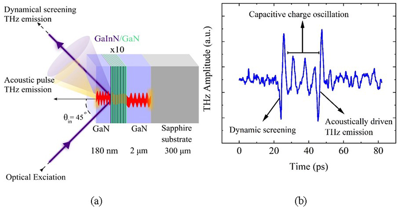
Figure 2 (a) MQWs sandwiched by the GaN layers are examined by free-space THz emission spectroscopy. (b) Typical terahertz emission waveform from MQW samples. Credit: Osaka University
The specialist team organised for THz emission spectroscopy, opto-THz science and wide-bandgap/quantum-well semiconductor material science has made a significant step towards 3D dynamic characterisation, including buried active layers in various materials and devices. “A 3D active tool to characterise ultrafast carrier dynamics, strain physics, phonon dynamics and ultrafast dielectric responses locally in a non-contact and non-destructive manner has become an essential area of research for new materials and devices. We hope the present work contributes to such an evolution”, says Professor Masayoshi Tonouchi.


 the original cross before corrosion removal, (b) the final terahertz image after post-processing and (c) the cross after corrosion removal. Credit: Georgia Tech-Lorraine")
